| CPC H01L 33/62 (2013.01) [H01L 33/005 (2013.01); H01L 33/42 (2013.01); H01L 33/486 (2013.01); H01L 2933/0016 (2013.01); H01L 2933/0066 (2013.01)] | 23 Claims |
|
1. A display device including at least one emission area emitting light and a transmission area adjacent to the at least one emission area, an entirety of the transmission area does not emit light and transmits external light, the display device comprising:
a substrate;
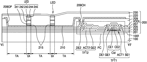
a circuit element including at least one transistor and a storage capacitor disposed on the substrate;
an insulating layer disposed on the circuit element and including a contact hole;
a first transparent electrode disposed on the insulating layer and electrically connected to the circuit element through the contact hole; and
at least one light-emitting diode disposed on the first transparent electrode and defining the at least one emission area, the at least one light-emitting diode comprising a PN diode including inorganic semiconductor based-materials,
wherein a portion of the first transparent electrode is located in the transmission area.
|