| CPC H01L 33/62 (2013.01) [H01L 33/382 (2013.01); H01L 33/486 (2013.01); H01L 33/54 (2013.01)] | 19 Claims |
|
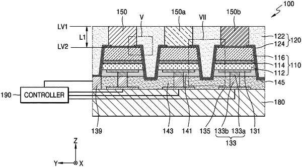
19. A semiconductor light-emitting device, comprising:
a circuit substrate connected to a controller;
a plurality of light-emitting device structures on the circuit substrate and separated from each other;
a partition wall structure between two adjacent light-emitting device structures of the plurality of light-emitting device structures, the partition wall structure defining a pixel space; and
an encapsulation layer in contact with an upper surface of each of the plurality of light-emitting device structures and a sidewall of the partition wall structure,
wherein each of the plurality of light-emitting device structures includes:
a first conductivity type semiconductor layer on the circuit substrate,
an active layer on the first conductivity type semiconductor layer,
a second conductivity type semiconductor layer on the active layer,
a first electrode connected to the first conductivity type semiconductor layer, and
a second electrode connected to the second conductivity type semiconductor layer,
wherein side surfaces of the first conductivity type semiconductor layer, the active layer, and the second conductivity type semiconductor layer are coated with an insulating layer,
wherein the partition wall structure includes an electrical conductor and vertically extends along the side surfaces of the first conductivity type semiconductor layer, the active layer, and the second conductivity type semiconductor layer with the insulating layer therebetween,
wherein the partition wall structure is continuous with the second electrode of each of adjacent light-emitting device structures of the plurality of light-emitting structures, the second electrode of each of the plurality of light-emitting device structures being continuous with the electrical conductor and extending through the insulating layer to contact the second conductivity type semiconductor layer,
wherein an upper surface of the partition wall structure is farther from the circuit substrate than an upper surface of the second conductivity type semiconductor layer is, and a lower surface of the partition wall structure is closer to the circuit substrate than a lower surface of the first conductivity type semiconductor layer is, and
wherein the partition wall structure surrounds each of the plurality of light-emitting device structures with the insulating layer therebetween.
|