| CPC H01L 33/382 (2013.01) [H01L 33/0095 (2013.01); H01L 33/54 (2013.01); H01L 2933/005 (2013.01); H01L 2933/0016 (2013.01)] | 12 Claims |
|
9. A method of manufacturing a display device, the method comprising:
providing a pixel in each pixel area on a substrate, the providing the pixel comprising:
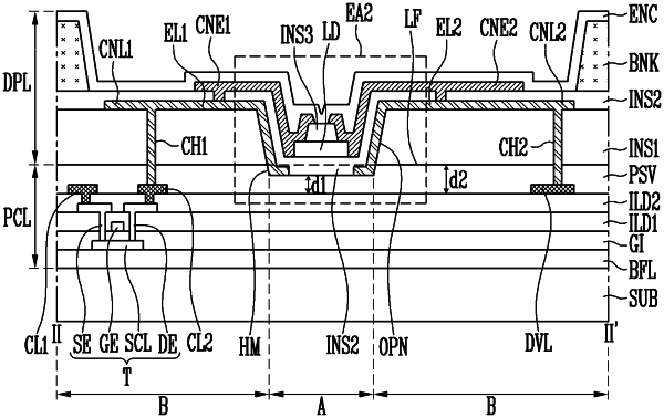
forming a transistor and a driving voltage line on the substrate;
forming a first insulating material layer on the transistor and the driving voltage line;
forming an insulating pattern having a sub opening exposing the first insulating material layer by forming a second insulating material layer on the first insulating material layer and removing a portion of the second insulating material layer;
forming a passivation layer having a groove and an insulating layer having an opening with a width greater than a width of the sub opening by removing a portion of the exposed first insulating material layer using the insulating pattern as an etching mask;
forming a first electrode and a second electrode spaced apart from each other on the insulating layer;
supplying light emitting elements to the pixel area and aligning the light emitting elements by forming an electric field between the first electrode and the second electrode by applying an alignment signal corresponding to each of the first and second electrodes; and
forming a contact electrode on each of the first and second electrodes.
|