| CPC H01L 31/107 (2013.01) [C30B 25/18 (2013.01); H01L 27/14636 (2013.01); H01L 31/02027 (2013.01); H04N 25/76 (2023.01)] | 20 Claims |
|
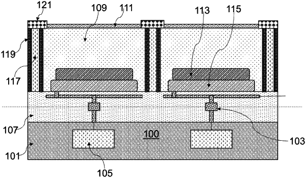
1. A single photon avalanche diode device comprising:
a logic substrate comprising an upper surface;
a sensor substrate bonded to the upper surface of the logic substrate, the sensor substrate comprising a pixel, the pixel comprising:
a passivation material comprising an opening;
an anti-reflective material overlying the passivation material;
an implanted p-type material;
an implanted n-type material; and
a junction region configured from the implanted p-type material and the implanted n-type material; and
a deep trench region bordering the pixel;
a first contact region on a first side of the sensor substrate coupled to the implanted p-type material, the first contact region being at least partially exposed through the opening; and
a second contact region on a second side of the sensor substrate coupled to the implanted n-type material and the logic substrate.
|