| CPC H01L 31/0203 (2013.01) [H01L 21/78 (2013.01); H01L 31/02002 (2013.01); H01L 31/02005 (2013.01); H01L 31/0392 (2013.01); H01L 31/1876 (2013.01); H01L 31/1896 (2013.01)] | 20 Claims |
|
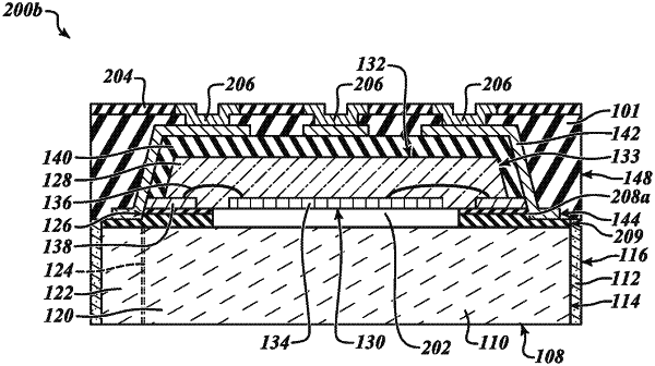
1. A device, comprising:
a transparent substrate including a first surface, a second surface opposite to the first surface in a direction directed from the first surface towards the second surface, and sidewalls transverse to the first surface and the second surface;
a molding compound on the sidewalls of the transparent substrate;
a die on the second surface of the transparent substrate, the die including:
a sensor aligned with the transparent substrate;
a contact that extends outward from an edge of the die and away from the sensor in a transverse direction transverse to the direction; and
an electrical connection having a first end coupled to the sensor and a second end coupled to the contact;
a first insulating layer on the die and on the contact of the die; and
a conductive layer on the first insulating layer, the conductive layer including:
a first end portion on the first insulating layer; and
a transverse portion on the first insulating layer, the transverse portion is transverse to the first end portion, is transverse to the contact, and is coupled to the contact.
|