| CPC H01L 29/7869 (2013.01) [H01L 29/22 (2013.01); H01L 29/66969 (2013.01)] | 14 Claims |
|
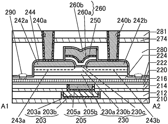
1. A semiconductor device comprising:
a first insulator;
a second insulator over the first insulator;
an oxide over the second insulator;
a first conductor and a second conductor apart from each other over the oxide;
a third insulator over the oxide, the first conductor, and the second conductor;
a third conductor over the third insulator and at least partly overlapping with a region between the first conductor and the second conductor;
a fourth insulator covering the oxide, the first conductor, the second conductor, the third insulator, and the third conductor;
a fifth insulator over the fourth insulator;
a sixth insulator over the fifth insulator;
a seventh insulator; and
an eighth insulator,
wherein the seventh insulator is in contact with an upper surface of the first conductor, a bottom surface of the fourth insulator, a side surface of the first conductor, a first side surface of the oxide,
wherein the eighth insulator is in contact with an upper surface of the second conductor, the bottom surface of the fourth insulator, a side surface of the second conductor, a first side surface of the oxide,
wherein an opening reaching the second insulator is formed in part of the fourth insulator, and
wherein the fifth insulator is in contact with the second insulator through the opening.
|