| CPC H01L 29/78681 (2013.01) [H01L 29/0669 (2013.01); H01L 29/20 (2013.01); H01L 29/42384 (2013.01); H01L 29/66742 (2013.01)] | 20 Claims |
|
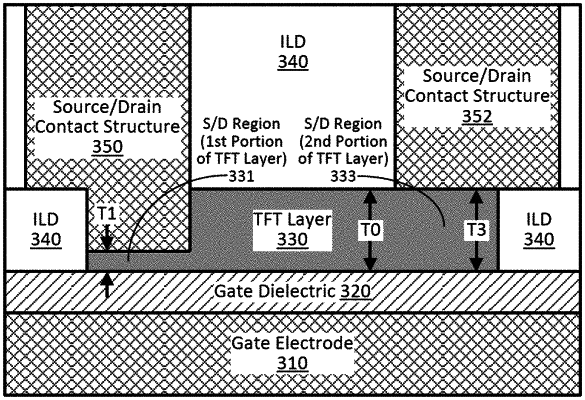
1. A transistor comprising:
a gate electrode including one or more metals;
a gate dielectric on the gate electrode;
a layer on the gate dielectric, the layer including one or more metals, the layer also including oxygen;
a first contact structure on the layer, the first contact structure including one or more metals, a first portion of the layer between the first contact structure and the gate dielectric; and
a second contact structure on the layer, the second contact structure including one or more metals, a second portion of the layer between the second contact structure and the gate dielectric, wherein the first portion of the layer has a first thickness, the second portion of the layer has a second thickness, and a third portion of the layer between the first and second portions of the layer has a third thickness, the third thickness greater than the first thickness, and the third thickness the same as the second thickness.
|