| CPC H01L 29/66545 (2013.01) [H01L 21/02603 (2013.01); H01L 21/76224 (2013.01); H01L 21/76802 (2013.01); H01L 29/0673 (2013.01); H01L 29/165 (2013.01); H01L 29/42356 (2013.01); H01L 29/7846 (2013.01); H01L 29/7848 (2013.01)] | 19 Claims |
|
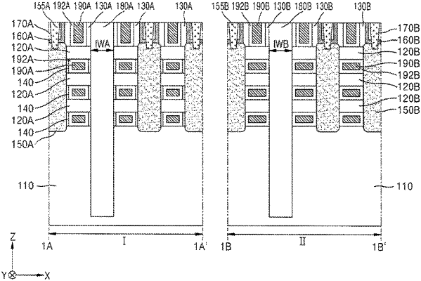
1. A semiconductor device, comprising:
a substrate extending in a first direction and a second direction that intersect with each other;
an isolation layer extending in the first direction;
gate electrodes on opposite sides of the isolation layer, the gate electrodes having a pair of external spacers on respective opposite sides of each of the gate electrodes;
nanowires on the substrate and spaced apart from each other in the second direction;
a gate dielectric layer between the nanowires and the gate electrodes;
source/drain regions spaced apart from the isolation layer with the nanowires interposed therebetween; and
respective source/drain contacts extending in a third direction perpendicular to an upper surface of the substrate and in contact with the source/drain regions,
wherein:
the gate electrodes extend in the first direction and are spaced apart from each other in the second direction, and surround the nanowires so that the gate electrodes are superimposed vertically with the nanowires,
the pair of external spacers includes a first external spacer in contact with the isolation layer, and a second external spacer spaced apart from the isolation layer, a width of the first external spacer being smaller than a width of the second external spacer in the second direction, and
the nanowires are in direct contact with the isolation layer.
|