| CPC H01L 29/512 (2013.01) [H01L 21/823431 (2013.01); H01L 27/0886 (2013.01); H01L 29/42392 (2013.01); H01L 29/517 (2013.01); H01L 29/66795 (2013.01); H01L 29/7851 (2013.01)] | 11 Claims |
|
1. An integrated circuit structure, comprising:
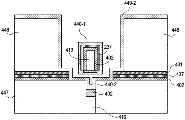
a fin extending from a substrate, the fin comprising a hanging fin region, which comprises a channel region, source and drain regions on opposite sides of the channel region, and a sub-fin region under the channel region between the source and drain regions, where the channel region and the sub-fin region are spaced apart;
a first isolation region adjacent both sides the sub-fin region beneath a second isolation region, wherein the second isolation region includes a trench in which the channel region is located;
a gate dielectric stack, comprising: i) a low-k material conformal to a top surface of the first isolation region and to sides and top of the channel region; ii) a first high-k material conformal to the low-k material over the first isolation region and on sides and top of the channel region; and iii) a second high-k material comprising a first portion and a second portion, wherein the first portion of the second high-k material is over the first high-k material on all four sides of the channel region, and the second portion of the second high-k material is conformal to a top surface of the second isolation region, conformal to sides and bottom of the trench, and conformal to a top of the sub-fin region; and
a gate electrode fills the trench and surrounds the second portion of the second high-k material around a perimeter of the channel region.
|