| CPC H01L 29/4236 (2013.01) [H01L 29/47 (2013.01); H01L 29/7813 (2013.01)] | 20 Claims |
|
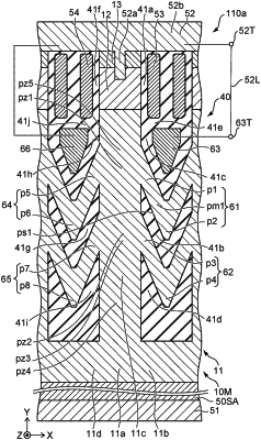
1. A semiconductor device, comprising:
a first electrode;
a second electrode including a first electrode portion, a direction from the first electrode toward the first electrode portion being along a first direction;
a third electrode, a direction from the first electrode toward the third electrode being along the first direction;
a semiconductor member including a first semiconductor region of a first conductivity type,
the first semiconductor region including a first partial region, a second partial region, and a third partial region,
the first partial region being between the first electrode and the first electrode portion,
the second partial region being between the first electrode and the third electrode,
a direction from the first partial region toward the second partial region being along a second direction crossing the first direction,
the third partial region being between the first partial region and the first electrode portion,
the third partial region including a first position and a second position,
the second position being between the first partial region and the first position;
a first conductive member including a first portion and a second portion,
the first portion being between the second partial region and the third electrode in the first direction,
the first portion being connected with the first position,
the second portion being connected with the first portion,
a position in the first direction of the second portion being between a position in the first direction of the first portion and a position in the first direction of the second partial region; and
an insulating part region including a first insulating region and a second insulating region,
the first insulating region being between the third electrode and a portion of the semiconductor member in the second direction,
the second insulating region being between the second position and the first electrode in the first direction,
the second insulating region being between the second position and the second portion in the second direction.
|