| CPC H01L 29/4236 (2013.01) [H01L 29/49 (2013.01); H10B 12/053 (2023.02); H10B 12/34 (2023.02); H10B 12/488 (2023.02); H10B 12/30 (2023.02); H10B 12/315 (2023.02)] | 20 Claims |
|
1. A semiconductor device, comprising:
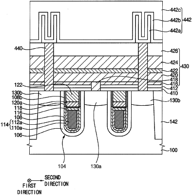
a substrate having a recess;
a gate insulation layer on a surface of the recess;
an impurity barrier layer on a surface of the gate insulation layer, the impurity barrier layer covering the surface of the gate insulation layer, the impurity barrier layer having a concentration of nitrogen greater than a concentration of nitrogen included in the gate insulation layer;
a first gate pattern on the impurity barrier layer, the first gate pattern filling a lower portion of the recess;
a second gate pattern on the first gate pattern and in the recess, the second gate pattern including a material different from materials included in the first gate pattern;
a capping insulation pattern on the second gate pattern, the capping insulation pattern filling the recess, the impurity barrier layer extending between the capping insulation pattern and the gate insulation layer; and
impurity regions at the substrate adjacent to an upper sidewall of the recess.
|