| CPC H01L 29/1095 (2013.01) [H01L 29/6656 (2013.01); H01L 29/66636 (2013.01)] | 15 Claims |
|
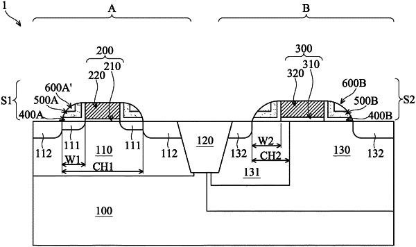
1. A method for forming a semiconductor structure, comprising:
providing a substrate comprising a first region and a second region;
forming a first gate structure on the first region;
forming a second gate structure on the second region;
sequentially forming a first dielectric layer, a second dielectric layer, and a third dielectric layer to cover the first gate structure and the second gate structure;
patterning the third dielectric layer to form a first portion of the third dielectric layer and a second portion of the third dielectric layer in the first region and the second region, respectively;
covering the second portion and partially removing the first portion of the third dielectric layer to form a first etching mask;
patterning the second dielectric layer by using the first etching mask and the second portion of the third dielectric layer as a second etching mask, to expose a portion of the first dielectric layer;
removing the portion of the first dielectric layer to form a first stacked spacer and a second stacked spacer on sidewalls of the first gate structure and the second gate structure, respectively;
wherein a width of the first stacked spacer is smaller than a width of the second stacked spacer.
|