| CPC H01L 29/0638 (2013.01) [G11C 16/0483 (2013.01); G11C 16/16 (2013.01); H01L 29/42328 (2013.01); H01L 29/42344 (2013.01); H01L 29/66825 (2013.01); H01L 29/66833 (2013.01); H01L 29/7889 (2013.01); H01L 29/7926 (2013.01); H10B 41/10 (2023.02); H10B 41/27 (2023.02); H10B 41/35 (2023.02); H10B 41/41 (2023.02); H10B 43/10 (2023.02); H10B 43/27 (2023.02); H10B 43/35 (2023.02); H10B 43/40 (2023.02)] | 20 Claims |
|
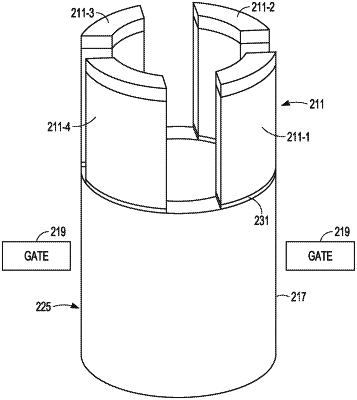
1. A memory device comprising:
a pillar disposed vertically as part of a memory array;
multiple transistors arranged along the pillar, with the pillar including a channel structure for each transistor of the multiple transistors;
a data line; and
a dissected contact between the data line and the channel structure, the dissected contact having one or more conductive regions contacting the channel structure and one or more non-conductive regions contacting the channel structure.
|