| CPC H01L 27/14634 (2013.01) [H01L 27/1469 (2013.01); H01L 27/14607 (2013.01); H01L 27/14636 (2013.01); H01L 27/14806 (2013.01)] | 30 Claims |
|
1. A semiconductor device comprising:
a first chip and a second chip, the first chip and the second chip being stacked on top of each other, the first chip having a first area, in which a plurality of first cells are arranged in matrix, the second chip having a second area, in which an electric circuit is arranged,
wherein a plurality of wiring lines electrically connects the first chip and the second chip, each of the plurality of wiring lines includes a bonding portion for bonding one of a plurality of conductive patterns placed in the first chip and one of a plurality of conductive patterns placed in the second chip,
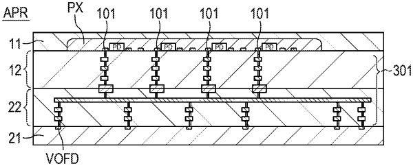
wherein the plurality of first cells each includes a photoelectric converter, a charge detector which detects an electric charge of the photoelectric converter, a transfer gate which transfers an electric charge of the photoelectric converter to the charge detector, and a reset transistor which resets an electric potential of the charge detector,
wherein the number of bonding portions included in a first wiring line out of the plurality of wiring lines is larger than the number of bonding portions included in a second wiring line out of the plurality of wiring lines,
wherein at least one of the bonding portions included in the first wiring line and the bonding portions included in the second wiring line is arranged in an overlap area, in which the first area and the second area overlap, and
wherein the first wiring line is connected to one of a source and a drain of the reset transistor.
|