| CPC H01L 27/14612 (2013.01) [H01L 27/146 (2013.01); H01L 27/1464 (2013.01); H01L 27/14641 (2013.01); H01L 27/14647 (2013.01); H01L 27/14667 (2013.01); H04N 25/59 (2023.01); H04N 25/76 (2023.01); H04N 25/77 (2023.01); H04N 25/771 (2023.01); H04N 23/62 (2023.01); H04N 25/50 (2023.01); H10K 39/32 (2023.02)] | 20 Claims |
|
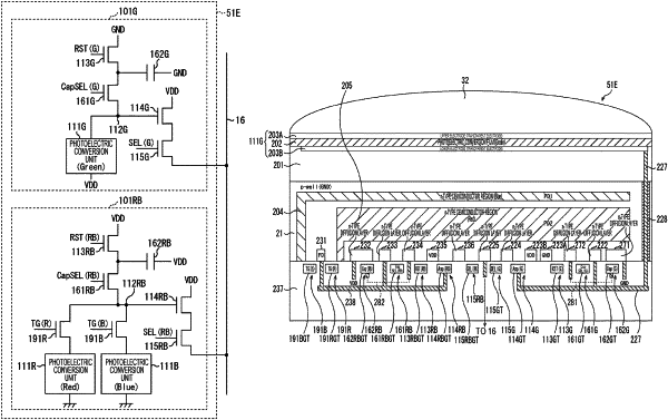
1. A solid-state image sensing device comprising:
a photoelectric conversion unit formed outside a semiconductor substrate;
a charge holding unit for holding signal charges generated by the photoelectric conversion unit;
a reset transistor for resetting a potential of the charge holding unit;
a capacitance switching transistor connected to the charge holding unit and directed for switching a capacitance of the charge holding unit;
an additional capacitance device connected to the capacitance switching transistor; and
a photodiode formed in the semiconductor substrate,
wherein, in a plan view, the capacitance switching transistor overlaps the photodiode.
|
|
11. An electronic device comprising a solid-state image sensing device, the solid-state image sensing device comprising a pixel having:
a photoelectric conversion unit formed outside a semiconductor substrate;
a charge holding unit for holding signal charges generated by the photoelectric conversion unit;
a reset transistor for resetting a potential of the charge holding unit;
a capacitance switching transistor connected to the charge holding unit and directed for switching a capacitance of the charge holding unit;
an additional capacitance device connected to the capacitance switching transistor; and
a photodiode formed in the semiconductor substrate,
wherein, in a plan view, the capacitance switching transistor overlaps the photodiode.
|