| CPC H01L 27/1461 (2013.01) [H01L 27/1462 (2013.01); H01L 27/1463 (2013.01); H01L 27/14621 (2013.01); H01L 27/14623 (2013.01); H01L 27/14627 (2013.01); H01L 27/14636 (2013.01); H01L 27/14645 (2013.01); H01L 27/14685 (2013.01); H01L 27/14689 (2013.01)] | 15 Claims |
|
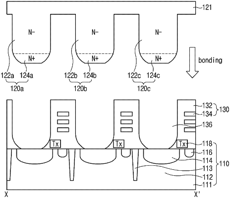
1. A method for forming an image sensing device comprising:
forming a first impurity region and a second impurity region in a first substrate;
forming a switching element over the first substrate, the switching element coupled to the first impurity region and the second impurity region;
forming an insulation structure over the first substrate to cover the switching element;
forming a trench exposing the first impurity region by etching the insulation structure; and
placing a photoelectric conversion element in the trench to couple the photoelectric conversion element to the first impurity region, the photoelectric conversion element disposed in a second substrate different from the first substrate and having a shape corresponding to a shape of the trench.
|