| CPC H01L 27/124 (2013.01) [G02F 1/13452 (2013.01); H01L 23/528 (2013.01); H01L 27/0207 (2013.01); H10K 59/131 (2023.02); H05K 1/118 (2013.01); H05K 1/189 (2013.01); H05K 3/323 (2013.01)] | 19 Claims |
|
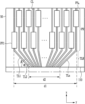
1. A display device comprising:
a substrate;
a circuit board;
pixels positioned on the substrate;
connecting lines;
pads electrically connected through the connecting lines to the pixels, positioned between the pixels and an edge of the substrate, and including a first pad and a second pad; and
conductive lines electrically connected through the pads to the connecting lines and including a first conductive line and a second conductive line,
wherein the first conductive line comprises a first first-line section and a second first-line section,
wherein the first first-line section is positioned closer to the edge of the substrate than the first pad,
wherein the second first-line section is positioned closer to the edge of the substrate than the first first-line section and is electrically connected through the first first-line section to the first pad,
wherein the second conductive line comprises a first second-line section and a second second-line section,
wherein the first second-line section is positioned closer to the edge of the substrate than the second pad,
wherein the second second-line section is positioned closer to the edge of the substrate than the first second-line section and is electrically connected through the first second-line section to the second pad,
wherein a minimum distance between the first first-line section and the first second-line section is larger than a minimum distance between the second first-line section and the second second-line section,
wherein the first first-line section and the first second-line section respectively directly contact the first pad and the second pad,
wherein the second first-line section and the second second-line section are respectively directly connected to the first first-line section and the first second-line section,
wherein each of the second first-line section and the second second-line section directly contacts the edge of the substrate, and
wherein the circuit board overlaps each of the first pad, the second pad, the first first-line section, the second first-line section, the first second-line section, and the second second-line section.
|