| CPC H01L 27/1207 (2013.01) [H03K 3/012 (2013.01); H03K 3/35613 (2013.01); H03K 19/0013 (2013.01); H03K 19/018528 (2013.01)] | 10 Claims |
|
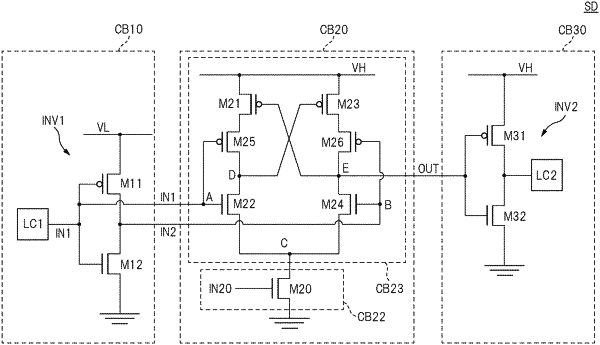
6. A semiconductor device comprising:
a first circuit connected between a first power supply line and a ground line;
a second circuit connected between a second power supply line and the ground line, wherein the second circuit receives a signal from the first circuit; and
a third circuit connected between a third power supply line and the ground line, wherein the third circuit receives a signal from the second circuit,
wherein the second circuit comprises a logic circuit and a switch element that are serially connected between the second power supply line and the ground line,
wherein the logic circuit comprises a first transistor of a first conductive type,
wherein the switch element comprises a second transistor of the first conductive type,
wherein the first transistor is formed in a semiconductor layer formed on a buried insulating layer, the buried insulating layer being formed on a support substrate,
wherein the second transistor includes a gate insulating film formed on a main surface of the support substrate, and
wherein the first transistor has a first channel formation region in the semiconductor layer, the second transistor has a second channel formation region in the support substrate, and an impurity concentration of the second channel formation region is higher than an impurity concentration of the first channel formation region.
|