| CPC H01L 27/0255 (2013.01) | 21 Claims |
|
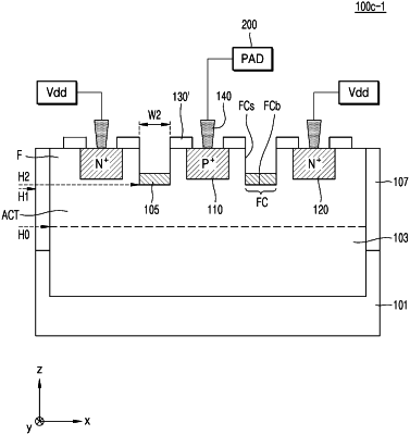
1. An electrostatic discharge (ESD) device comprising:
a well formed in a substrate, the well having a first conductive type and a first doping concentration;
an active region formed at an upper portion of the substrate, the active region having a second doping concentration higher than the first doping concentration;
a plurality of fins extending in a first direction across the well in a protruding manner from the substrate, the plurality of fins being spaced apart from one another in a second direction perpendicular to the first direction;
a first conductive impurity region formed by doping a portion of each of the plurality of fins with first conductive impurities;
a second conductive impurity region formed by doping a portion of each of the plurality of fins with second conductive impurities having a second conductive type different from the first conductive type, the second conductive impurity region being disposed apart from the first conductive impurity region in the first direction; and
a fin-cut isolation region disposed between the first conductive impurity region and the second conductive impurity region in the first direction in each of the plurality of fins to cut each of the plurality of fins into at least a first fin portion and a second fin portion,
wherein a bottom surface of the fin-cut isolation region is higher than a bottom surface of the active region.
|