| CPC H01L 25/0657 (2013.01) [H01L 23/3128 (2013.01); H01L 25/18 (2013.01); H01L 2225/06513 (2013.01); H01L 2225/06517 (2013.01); H01L 2225/06541 (2013.01); H01L 2225/06586 (2013.01)] | 20 Claims |
|
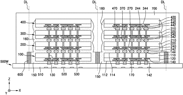
1. A method of manufacturing a semiconductor package, the method comprising:
preparing a base substrate including a semiconductor chip mounting region;
forming a dam structure on the base substrate, the dam structure surrounding the semiconductor chip mounting region;
mounting a first semiconductor chip on the semiconductor chip mounting region of the base substrate, the first semiconductor chip having a first non-conductive film attached thereto;
applying a pressure to the first semiconductor chip such that the first non-conductive film is in contact with the dam structure;
stacking a second semiconductor chip on the first semiconductor chip, the second semiconductor chip having a second non-conductive film attached thereto; and
forming a molding member covering the base substrate, the first semiconductor chip, and the second semiconductor chip.
|