| CPC H01L 25/0657 (2013.01) [H01L 23/16 (2013.01); H01L 23/3185 (2013.01); H01L 23/49811 (2013.01); H01L 24/16 (2013.01); H01L 24/48 (2013.01); H01L 2224/16227 (2013.01); H01L 2224/48227 (2013.01)] | 20 Claims |
|
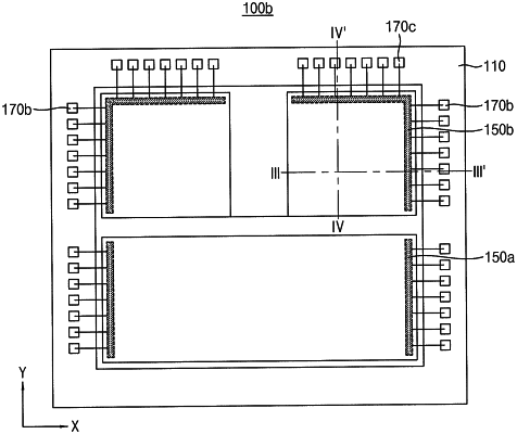
1. A semiconductor package, comprising:
a substrate including a plurality of interconnections;
at least one chip on the substrate;
a plurality of first pads on the substrate, the plurality of first pads overlapping the at least one chip;
a plurality of bumps between the substrate and the at least one chip;
a plurality of second pads on an edge portion of a first side of the substrate, the plurality of second pads being electrically connected to the at least one chip through a plurality of first conductive wires;
an underfill that fills a space between the substrate and the at least one chip; and
a first dam on the substrate, the first dam overlapping the at least one chip.
|