| CPC H01L 24/82 (2013.01) [H01L 23/5389 (2013.01); H01L 24/02 (2013.01); H01L 24/16 (2013.01); H01L 24/19 (2013.01); H01L 24/20 (2013.01); H01L 24/24 (2013.01); H01L 24/25 (2013.01); H01L 25/105 (2013.01); H01L 25/18 (2013.01); H01L 25/50 (2013.01); H01L 2224/0239 (2013.01); H01L 2224/02313 (2013.01); H01L 2224/04105 (2013.01); H01L 2224/12105 (2013.01); H01L 2224/13024 (2013.01); H01L 2224/16227 (2013.01); H01L 2224/18 (2013.01); H01L 2224/245 (2013.01); H01L 2224/24011 (2013.01); H01L 2224/24137 (2013.01); H01L 2224/25171 (2013.01); H01L 2224/32145 (2013.01); H01L 2224/32225 (2013.01); H01L 2224/73265 (2013.01); H01L 2224/73267 (2013.01); H01L 2224/82106 (2013.01); H01L 2224/92244 (2013.01); H01L 2224/97 (2013.01); H01L 2225/0651 (2013.01); H01L 2225/06568 (2013.01); H01L 2225/1035 (2013.01); H01L 2225/1041 (2013.01); H01L 2225/1058 (2013.01); H01L 2924/01029 (2013.01); H01L 2924/15313 (2013.01)] | 20 Claims |
|
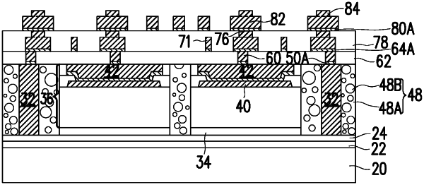
1. A method comprising:
encapsulating a device die in an encapsulating material;
planarizing the encapsulating material and the device die;
forming a conductive feature over and electrically coupling to the device die, wherein the forming the conductive feature comprises:
forming an adhesion layer;
forming a metal region over the adhesion layer, wherein parts of the adhesion layer and the metal region form a metal line; and
after the metal region is formed, forming a via over the metal line; and
after the conductive feature is formed, performing a re-etching process, wherein in the re-etching process, the metal region is etched faster than the adhesion layer, wherein in the re-etching process, both of the metal line and the via are etched.
|