| CPC H01L 24/72 (2013.01) [H01L 2224/72 (2013.01); H01L 2924/01013 (2013.01); H01L 2924/01042 (2013.01); H01L 2924/1033 (2013.01); H01L 2924/10272 (2013.01)] | 21 Claims |
|
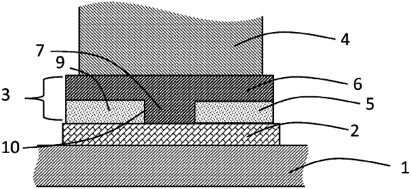
1. A power semiconductor module, comprising:
a base plate having a top surface and a bottom surface;
a semiconductor chip having a bottom surface and a top surface, the semiconductor chip being disposed on the top surface of the base plate, the bottom surface of the semiconductor chip being in contact with the top surface of the base plate, the semiconductor chip including a wide-bandgap semiconductor material;
a preform having a bottom surface and a top surface, the preform being disposed on the top surface of the semiconductor chip, the bottom surface of the preform being in contact with the top surface of the semiconductor chip, the preform comprising a first electrically conductive layer and a second electrically conductive layer, wherein the first electrically conductive layer has a protrusion protruding towards the top surface of the semiconductor chip and defining at least one recess in the first electrically conductive layer of the preform, the protrusion and the first electrically conductive layer being made from the same material or from different materials, and wherein at least a portion of the second electrically conductive layer is positioned in the recess and on the top surface of the semiconductor chip, the material of the protrusion having a higher melting point than the material of the second electrically conductive layer; and
a pressing element in contact with the top surface of the preform and configured to apply a pressure onto the top surface of the preform, wherein the power semiconductor module is configured so that in an event of semiconductor chip failure with heat dissipation causing the semiconductor chip to be defective, the protrusion of the first electrically conductive layer penetrates through residual material of the semiconductor chip upon pressure applied by the pressing element towards the base plate so as to establish a contact between the protrusion of the first electrically conductive layer and the base plate and form a short circuit bridging the defective semiconductor chip in a short circuit failure mode.
|