| CPC H01L 24/14 (2013.01) [H01L 23/16 (2013.01); H01L 23/28 (2013.01); H01L 23/49816 (2013.01); H01L 23/5384 (2013.01); H01L 23/562 (2013.01); H01L 23/3128 (2013.01); H01L 2224/16225 (2013.01); H01L 2224/18 (2013.01); H01L 2224/32225 (2013.01); H01L 2224/73204 (2013.01); H01L 2924/1431 (2013.01); H01L 2924/1433 (2013.01); H01L 2924/1436 (2013.01); H01L 2924/181 (2013.01); H01L 2924/3511 (2013.01)] | 16 Claims |
|
1. A semiconductor package comprising:
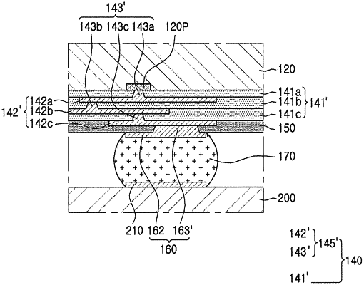
a connection member having a first surface and a second surface opposing each other in a stacking direction of the semiconductor package and including an insulating member and a plurality of redistribution layers disposed on different levels in the insulating member in the stacking direction, the plurality of redistribution layers having a plurality of wiring patterns adjacent to the second surface and a plurality of redistribution vias connected to the plurality of wiring patterns, respectively;
a semiconductor chip disposed on the first surface of the connection member and having connection pads connected to the plurality of redistribution layers;
an encapsulant disposed on the first surface of the connection member and encapsulating the semiconductor chip;
an insulation layer disposed on the second surface of the connection member;
a plurality of underbump metallurgy (UBM) pads disposed on the insulation layer; and
a plurality of UBM vias connecting the plurality of UBM pads to the plurality of wiring patterns through the insulation layer, and none of the UBM vias overlap any of the plurality of redistribution vias on the different levels,
wherein each of the plurality of wiring patterns has a thickness of 0.5 μm to 15 μm, and
wherein each of the plurality of UBM vias has a first width in a first direction referring to a diameter direction of a corresponding UBM pad and a second width in a second direction perpendicular to the first direction, and the second width is greater than the first width.
|