| CPC H01L 23/49838 (2013.01) [H01L 23/13 (2013.01); H01L 24/16 (2013.01); H05K 1/0296 (2013.01); H05K 1/115 (2013.01); H05K 1/181 (2013.01); H01L 2224/16227 (2013.01)] | 19 Claims |
|
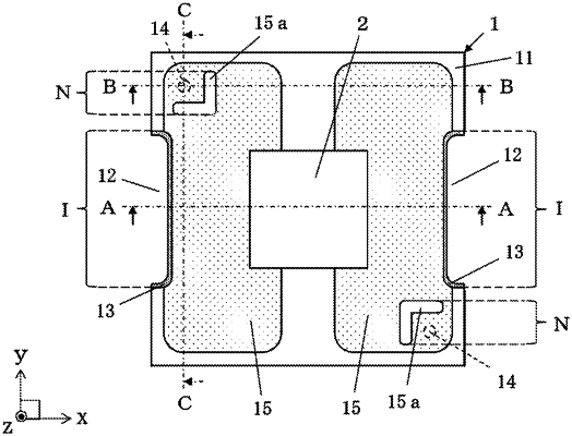
1. A wiring substrate comprising:
an insulating substrate that is shaped in a quadrangle that extends along a X direction and a Y direction in a plan view, including a mounting portion where an electronic component is mounted on a side of a principal surface of the insulating substrate, and having a recess on a side surface wherein when viewed from the X direction, the recess is at a position overlapping the mounting portion;
an inner surface electrode which is located on an inner surface of the recess;
a via conductor which is located on a corner side of the insulating substrate in a perspective plan view and has both ends located in a thickness direction of the insulating substrate; and
a wiring conductor, on the side of the principal surface of the insulating substrate, connecting the mounting portion, the inner surface electrode, and the via conductor with each other,
wherein, in the perspective plan view, the wiring conductor has a wiring conductor absent region which surrounds a region located between the mounting portion and the via conductor, wherein the wiring conductor absent region is on the insulating substrate where the wiring conductor is not positioned and is surrounded by the wiring conductor when viewed from the thickness direction
wherein when viewed from the X direction, the recess is positioned to not overlap with the wiring conductor absent region.
|