| CPC H01L 23/49827 (2013.01) [H01L 21/486 (2013.01); H01L 23/12 (2013.01); H01L 23/49816 (2013.01); H01L 23/49833 (2013.01); H01L 23/49838 (2013.01); H01L 23/5384 (2013.01); H01L 23/5386 (2013.01); H01L 24/16 (2013.01); H01L 24/48 (2013.01); H01L 24/73 (2013.01); H01L 25/0652 (2013.01); H01L 25/0657 (2013.01); H01L 25/16 (2013.01); H01L 28/10 (2013.01); H01L 28/40 (2013.01); H01L 28/60 (2013.01); H05K 1/11 (2013.01); H05K 3/28 (2013.01); H01L 2224/16227 (2013.01); H01L 2224/48091 (2013.01); H01L 2224/48106 (2013.01); H01L 2224/48225 (2013.01); H01L 2224/73257 (2013.01); H01L 2225/0651 (2013.01); H01L 2225/06517 (2013.01); H01L 2225/06548 (2013.01); H01L 2225/06572 (2013.01); H01L 2924/19011 (2013.01); H01L 2924/19041 (2013.01); H01L 2924/19042 (2013.01)] | 15 Claims |
|
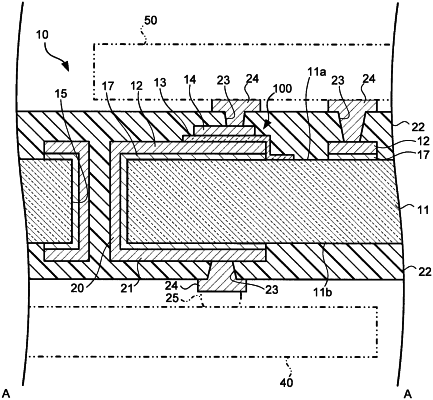
1. A through electrode substrate comprising:
a substrate having a first surface and a second surface facing the first surface;
a through electrode penetrating through the substrate; and
a capacitor including a first conductive layer, an insulating layer, and a second conductive layer, arranged on the first surface side of the substrate, and electrically connected with the through electrode,
wherein
the insulating layer includes a first part and a second part and is arranged on the first conductive layer,
the second conductive layer is arranged on the insulating layer,
the first part is arranged between the first conductive layer and the second conductive layer,
the second part covers at least a part of a side surface of the first conductive layer,
at least a part of the through electrode and the first conductive layer are integrated to form a structure, and
a part of an inner surface of the through electrode is covered with the insulating layer extending from the capacitor.
|