| CPC H01L 23/49822 (2013.01) [H01L 24/32 (2013.01); H01L 2224/32225 (2013.01); H01L 2924/3511 (2013.01)] | 6 Claims |
|
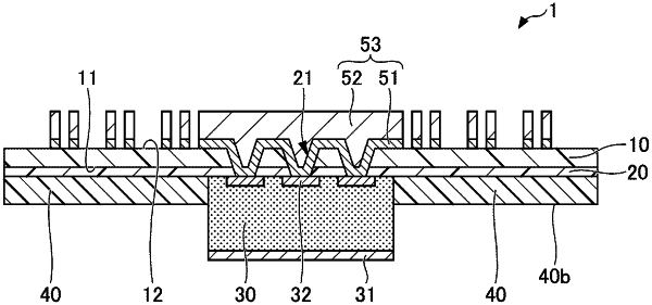
1. A semiconductor device comprising:
a film substrate;
an adhesive on a first surface of the film substrate;
an electronic component on the adhesive;
a wiring layer on a second surface of the film substrate opposite from the first surface, the wiring layer being connected to the electronic component through a via hole piercing through the film substrate and the adhesive; and
a reinforcement member in an area around the electronic component on the adhesive, the reinforcement member having a thickness smaller than a thickness of the electronic component.
|