| CPC H01L 23/3672 (2013.01) [H01L 21/4803 (2013.01); H01L 21/4882 (2013.01); H01L 23/043 (2013.01); H01L 23/051 (2013.01); H01L 23/3675 (2013.01); H01L 23/3738 (2013.01); H01L 31/0203 (2013.01); H01L 31/02325 (2013.01); H01S 5/02469 (2013.01); H01L 31/024 (2013.01); H01L 31/02327 (2013.01); H01L 33/483 (2013.01); H01L 33/58 (2013.01); H01L 33/641 (2013.01); H01L 33/642 (2013.01); H01L 2924/0002 (2013.01); H01L 2933/0075 (2013.01); H05K 1/0203 (2013.01); H05K 1/0274 (2013.01); H05K 1/0306 (2013.01); H05K 1/144 (2013.01); H05K 2201/041 (2013.01); H05K 2201/049 (2013.01); H05K 2201/09036 (2013.01); H05K 2201/09063 (2013.01); H05K 2201/09827 (2013.01); H05K 2201/10098 (2013.01); H05K 2201/10106 (2013.01); H05K 2201/10151 (2013.01); H05K 2201/10174 (2013.01)] | 7 Claims |
|
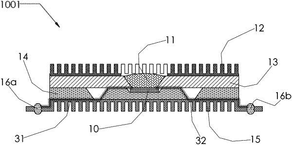
1. A device, comprising:
a first silicon cover plate having a first primary side and a second primary side opposite the first primary side thereof;
a second silicon cover plate having a first primary side and a second primary side opposite the first primary side thereof, the first primary side of the second silicon cover plate including an indentation configured to accommodate an electronic device therein, the first primary side of the second silicon cover plate configured to mate with the second primary side of the first silicon cover plate when the first silicon cover plate and the second silicon cover plate are joined together with the electronic device sandwiched therebetween;
a first silicon heat sink having a first primary side and a second primary side opposite the first primary side thereof, the first primary side of the first silicon heat sink configured to mate with the second primary side of the second silicon cover plate when the first silicon heat sink and the second silicon cover plate are joined together; and
a second silicon heat sink having a first primary side and a second primary side opposite the first primary side thereof, the second primary side of the second silicon heat sink configured to mate with the first primary side of the first silicon cover plate when the second silicon heat sink and the first silicon cover plate are joined together,
wherein the second primary side of the first silicon cover plate includes first and second metallic patterns deposited thereon and configured to electrically connect to first and second electrodes of the electronic device, respectively, when the first silicon cover plate and the second silicon cover plate are joined together with the electronic device sandwiched therebetween,
wherein the second silicon cover plate further includes first and second vias on first and second sides of the indentation, respectively, the first and the second vias filled with an electrically-conductive material and corresponding to the first and the second metallic patterns on the first silicon cover plate to electrically connect to the first and the second metallic patterns, respectively, when the first silicon cover plate and the second silicon cover plate are joined together with the electronic device sandwiched therebetween,
wherein the first primary side of the first silicon heat sink includes first and second electrodes deposited thereon and corresponding to the first and the second vias of the second silicon cover plate to electrically connect to the electrically-conductive material in the first and the second vias when the first silicon heat sink and the second silicon cover plate are joined together, and
wherein the second primary side of the second silicon cover plate includes third and fourth metallic patterns deposited thereon and configured to electrically connect to the first and the second electrodes of the first silicon heat sink, respectively, when the first silicon heat sink and the second silicon cover plate are joined together.
|