| CPC H01L 23/3121 (2013.01) [H01L 21/4853 (2013.01); H01L 21/565 (2013.01); H01L 21/78 (2013.01); H01L 23/49541 (2013.01)] | 27 Claims |
|
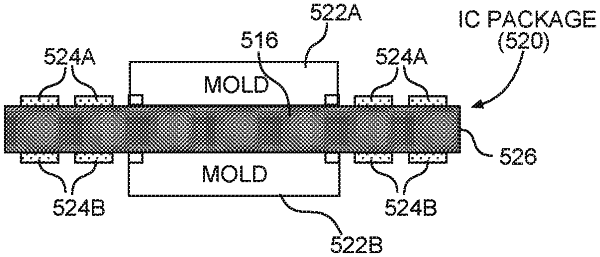
1. An integrated circuit (IC) package comprising:
a component
a mold material attached to a metallization structure and covering the component, the mold material having at least three sides comprising a first side, a second side, and a third side, each of the at least three sides perpendicular to the metallization structure
a first pad positioned adjacent to the first side;
a second pad positioned adjacent to the second side;
a third pad positioned adjacent to the third side such that each of the first pad, the second pad, and the third pad are not covered by the mold material; and
a mask remainder positioned on the top surface of the metallization structure, wherein there is no mask remainder on the component or on the first pad, second pad, or third pad.
|