| CPC H01L 23/3107 (2013.01) [H01L 21/561 (2013.01); H01L 21/568 (2013.01); H01L 21/6835 (2013.01); H01L 23/3114 (2013.01); H01L 23/3171 (2013.01); H01L 23/3185 (2013.01); H01L 23/552 (2013.01); H01L 23/60 (2013.01); H01L 24/19 (2013.01); H01L 23/3128 (2013.01); H01L 24/16 (2013.01); H01L 24/32 (2013.01); H01L 24/73 (2013.01); H01L 24/81 (2013.01); H01L 24/92 (2013.01); H01L 25/0655 (2013.01); H01L 2221/68345 (2013.01); H01L 2221/68359 (2013.01); H01L 2224/0401 (2013.01); H01L 2224/16227 (2013.01); H01L 2224/32225 (2013.01); H01L 2224/73204 (2013.01); H01L 2224/81005 (2013.01); H01L 2224/92125 (2013.01); H01L 2224/97 (2013.01); H01L 2924/014 (2013.01); H01L 2924/01015 (2013.01); H01L 2924/01082 (2013.01); H01L 2924/14 (2013.01); H01L 2924/1431 (2013.01); H01L 2924/1434 (2013.01); H01L 2924/15192 (2013.01); H01L 2924/15311 (2013.01); H01L 2924/15331 (2013.01); H01L 2924/3025 (2013.01)] | 20 Claims |
|
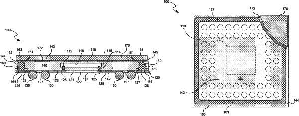
1. A packaged semiconductor device, comprising:
a redistribution structure having first side, a second side, a dielectric formation having a thickness from the first side to the second side, die contacts at the first side of the redistribution structure, at least one shield contact at the first side of the redistribution structure, and ball external pads at the second side of the redistribution structure;
a foundation deposited on the first side of the redistribution structure, wherein the foundation has openings and is spaced laterally apart from the outer perimeter of the semiconductor die, wherein the opening is configured to receive deposited conductive material;
a semiconductor die mounted on the first side of the redistribution structure, wherein the semiconductor die has an outer perimeter and is laterally offset from the foundation;
a conductive wall on the first side of the redistribution structure spaced laterally apart from the outer perimeter of the semiconductor die, wherein the conductive wall is in the openings of the foundation, electrically coupled to the shield contact, and extends around at least a portion of the outer perimeter of the semiconductor die;
an encapsulant covering at least a portion of the semiconductor die and extending laterally outward with respect to the outer perimeter of the semiconductor die; and
a conductive cap attached to the encapsulant and electrically coupled to the conductive wall such that the conductive wall and the conductive cap form a shield configured to protect the semiconductor die from electromagnetic interference.
|