US 11,742,236 B2
Structure and method for enhancing robustness of ESD device
Alexander Kalnitsky, San Francisco, CA (US); Jen-Chou Tseng, Jhudong Township (TW); Chia-Wei Hsu, New Taipei (TW); and Ming-Fu Tsai, Hsinchu (TW)
Assigned to TAIWAN SEMICONDUCTOR MANUFACTURING COMPANY LIMITED, Hsinchu (TW)
Filed by Taiwan Semiconductor Manufacturing Co., Ltd., Hsinchu (TW)
Filed on Nov. 30, 2020, as Appl. No. 17/106,553.
Application 17/106,553 is a division of application No. 16/021,200, filed on Jun. 28, 2018, granted, now 10,854,501.
Application 16/021,200 is a division of application No. 14/596,339, filed on Jan. 14, 2015, granted, now 10,026,640, issued on Jul. 17, 2018.
Claims priority of provisional application 62/065,200, filed on Oct. 17, 2014.
Prior Publication US 2021/0082743 A1, Mar. 18, 2021
Int. Cl. H01L 21/762 (2006.01); H01L 27/02 (2006.01); H01L 29/06 (2006.01); H01L 29/73 (2006.01); H01L 29/66 (2006.01)
CPC H01L 21/76224 (2013.01) [H01L 27/0259 (2013.01); H01L 29/0649 (2013.01); H01L 29/66234 (2013.01); H01L 29/73 (2013.01)] 20 Claims
OG exemplary drawing
 
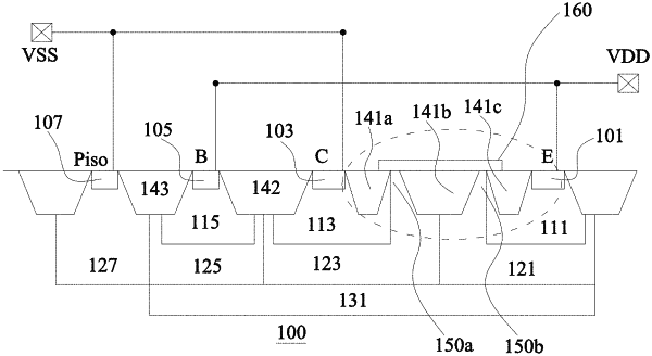
1. A device comprising:
a bipolar junction transistor comprising:
a base region connected to a power supply node;
an emitter region connected to the power supply node; and
a collector region between the emitter region and the base region, the collector region connected to a ground node; and
an isolation structure between the emitter region and the collector region, the isolation structure comprising a first partition structure extending substantially abreast at least one of the emitter region and the collector region.