| CPC H01L 21/67092 (2013.01) [H01L 21/6838 (2013.01); H01L 21/6875 (2013.01); H01L 21/68735 (2013.01); H01L 21/68742 (2013.01); H01L 21/68785 (2013.01)] | 19 Claims |
|
1. A method comprising:
mounting a first wafer on a first chuck;
mounting a second wafer on a second chuck;
cleaning the first wafer and the second wafer;
bonding the second wafer on the first wafer; and
performing a heat treatment process on the first wafer and the second wafer,
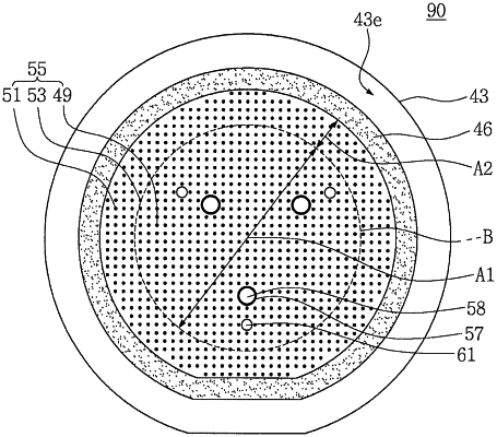
wherein the first chuck comprises a first base having a first region and a second region circumferentially surrounding the first region, a plurality of first lift holes passing through the first base first region, a plurality of first lift guard rings on the first base and surrounding the plurality of first lift holes, a plurality of first support pins extending outwardly from the first region of the base, wherein the plurality of first support pins have upper surfaces at a first level, and a plurality of second support pins extending outwardly from the second region of the base, wherein the plurality of second support pins have upper surfaces at a level lower than the first level, and
wherein each of the plurality of first lift guard rings has an upper surface at the first level.
|