| CPC H01L 21/4882 (2013.01) [H01L 21/4853 (2013.01); H01L 21/4857 (2013.01); H01L 21/565 (2013.01); H01L 23/3128 (2013.01); H01L 23/3675 (2013.01); H01L 23/5383 (2013.01); H01L 23/5386 (2013.01); H01L 23/5389 (2013.01); H01L 24/19 (2013.01); H01L 24/20 (2013.01); H01L 21/56 (2013.01); H01L 24/27 (2013.01); H01L 2224/214 (2013.01)] | 20 Claims |
|
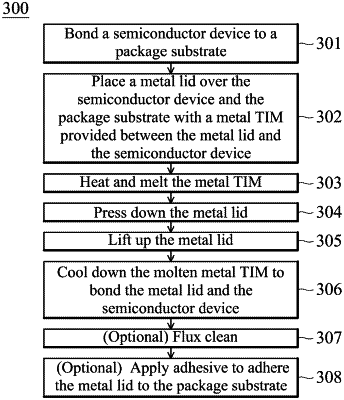
1. A method for forming a semiconductor device package, comprising:
bonding a semiconductor device to a first surface of a package substrate;
placing a metal lid over the semiconductor device and the package substrate with a metal thermal interface material (TIM) provided between the metal lid and a top surface of the semiconductor device;
heating the metal TIM to melt the metal TIM;
pressing the metal lid downward so that the molten metal TIM laterally flows toward a boundary of the semiconductor device along a first direction, and an outermost point of a lateral sidewall of the molten metal TIM extends beyond the boundary of the semiconductor device;
lifting the metal lid upward so that the molten metal TIM laterally flows toward a center of the top surface of the semiconductor device along a second direction opposite to the first direction, and the outermost point of the lateral sidewall of the molten metal TIM is within the boundary of the semiconductor device; and
bonding the metal lid to the semiconductor device through the metal TIM by cooling the molten metal TIM.
|