| CPC H01L 21/3247 (2013.01) [H01L 21/26506 (2013.01); H01L 21/7806 (2013.01)] | 16 Claims |
|
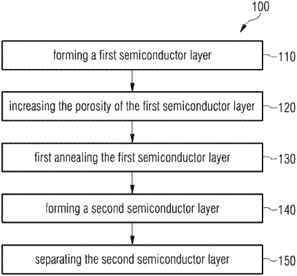
1. A method of forming a semiconductor device, the method comprising:
forming a first semiconductor layer on a semiconductor substrate, the first semiconductor layer being of the same dopant type as the semiconductor substrate, the first semiconductor layer having a higher dopant concentration than the semiconductor substrate;
increasing the porosity of the first semiconductor layer;
first annealing the first semiconductor layer at a temperature of at least 1050° C.;
forming a second semiconductor layer on the first semiconductor layer;
a second annealing in an atmosphere of hydrogen, the second annealing performed after the first annealing but before forming the second semiconductor layer; and
separating the second semiconductor layer from the semiconductor substrate by splitting within the first semiconductor layer.
|