US 11,742,208 B2
Method of reducing voids and seams in trench structures by forming semi-amorphous polysilicon
Damien Thomas Gilmore, Allen, TX (US); Jonathan P. Davis, Allen, TX (US); Azghar H Khazi-Syed, Arlington, TX (US); Shariq Arshad, Allen, TX (US); Khanh Quang Le, Garland, TX (US); Kaneez Eshaher Banu, Plano, TX (US); Jonathan Roy Garrett, Garland, TX (US); Sarah Elizabeth Bradshaw, Dallas, TX (US); and Eugene Clayton Davis, McKinney, TX (US)
Assigned to Texas Instruments Incorporated, Dallas, TX (US)
Filed by Texas Instruments Incorporated, Dallas, TX (US)
Filed on Mar. 25, 2020, as Appl. No. 16/829,862.
Prior Publication US 2021/0305050 A1, Sep. 30, 2021
Int. Cl. H01L 21/28 (2006.01); H01L 29/40 (2006.01); H01L 29/423 (2006.01); H01L 29/49 (2006.01)
CPC H01L 21/28035 (2013.01) [H01L 29/401 (2013.01); H01L 29/4236 (2013.01); H01L 29/4916 (2013.01)] 16 Claims
OG exemplary drawing
 
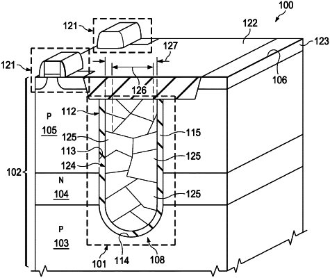
1. A microelectronic device, comprising:
a substrate;
a trench structure in the substrate, the trench structure including:
a trench in the substrate;
a seed layer in the trench, the seed layer including an amorphous dielectric material; and
a polysilicon core contacting the amorphous dielectric material, the polysilicon core filling the trench structure inside the seed layer, the polysilicon core having silicon grains, wherein an average size of the silicon grains is greater than half a minimum lateral dimension of the trench structure inside the seed layer.