US 11,742,201 B2
Method of filling gaps with carbon and nitrogen doped film
Wan-Yi Kao, Baoshan Township (TW); and Chung-Chi Ko, Nantou (TW)
Assigned to TAIWAN SEMICONDUCTOR MANUFACTURING COMPANY, LTD, Hsinchu (TW)
Filed by Taiwan Semiconductor Manufacturing Co., Ltd., Hsinchu (TW)
Filed on Dec. 23, 2021, as Appl. No. 17/645,867.
Application 17/645,867 is a continuation of application No. 16/529,098, filed on Aug. 1, 2019, granted, now 11,211,243.
Claims priority of provisional application 62/770,424, filed on Nov. 21, 2018.
Prior Publication US 2022/0122834 A1, Apr. 21, 2022
This patent is subject to a terminal disclaimer.
Int. Cl. C23C 16/56 (2006.01); H01L 21/02 (2006.01); C23C 16/04 (2006.01); C23C 16/40 (2006.01); C23C 16/455 (2006.01); H01L 21/762 (2006.01); H01L 21/8234 (2006.01); H01L 27/088 (2006.01); H01L 29/66 (2006.01); H01L 29/78 (2006.01)
CPC H01L 21/0228 (2013.01) [C23C 16/042 (2013.01); C23C 16/045 (2013.01); C23C 16/402 (2013.01); C23C 16/45527 (2013.01); C23C 16/45553 (2013.01); C23C 16/56 (2013.01); H01L 21/0214 (2013.01); H01L 21/76224 (2013.01); H01L 21/823431 (2013.01); H01L 21/823481 (2013.01); H01L 27/0886 (2013.01); H01L 29/6681 (2013.01); H01L 29/785 (2013.01)] 20 Claims
OG exemplary drawing
 
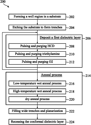
1. A method comprising:
depositing a dielectric layer; and
performing an anneal process on the dielectric layer, wherein the anneal process comprises:
a first wet anneal process performed at a first temperature;
a second wet anneal process performed at a second temperature higher than the first temperature; and
a dry anneal process performed at a third temperature higher than the first temperature.