| CPC H01J 37/3175 (2013.01) [H01J 37/3026 (2013.01); H01J 2237/31754 (2013.01); H01J 2237/31769 (2013.01)] | 12 Claims |
|
1. A proximity effect correcting method comprising:
calculating an energy distribution of a backscattered beam to be produced by backscattering of an electron beam in a substrate on a basis of drawing information input from outside and surface profile information of the substrate input from outside; and
calculating a required energy amount of the electron beam on a basis of the calculated energy distribution,
wherein
the drawing information is information for forming a pattern in a resist film on the substrate with irradiation of the electron beam,
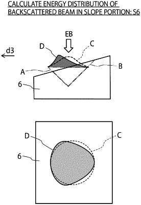
the surface profile information is information related to heights of the substrate having different heights in an irradiation direction of the electron beam,
the substrate comprises a first flat portion having a first height, and a second flat portion having a second height,
the surface profile information comprises first arrangement information indicating respective arrangement states of the first flat portion and the second flat portion, and height information indicating respective heights of the first flat portion and the second flat portion, and
the calculating of the energy distribution is based on the drawing information, the first arrangement information, the height information, an inclination angle of each of slope portions arranged on a surface of the substrate, and an inclination direction of each of the slope portions.
|