| CPC H01G 4/30 (2013.01) [H01G 4/012 (2013.01); H01G 4/1218 (2013.01)] | 23 Claims |
|
1. A multilayer ceramic electronic component, comprising:
a ceramic body comprising a dielectric layer; and
first and second internal electrodes disposed inside the ceramic body and disposed to oppose each other with the dielectric layer interposed therebetween,
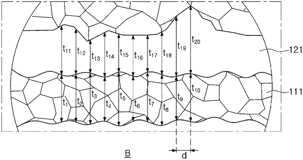
wherein, when an average thickness of the dielectric layer is referred to as td and a standard deviation of a thickness of the dielectric layer in each position is referred to as σtd, while an average thickness of the first and second internal electrodes is referred to as to and a standard deviation of a thickness of a pre-determined region of any layer of the internal electrodes in each position is referred to as σte, a ratio (σte/σtd) of the standard deviation of the internal electrodes in each position to the standard deviation of the thickness of the dielectric layer in each position satisfies 0σte/σtd≤1.35, and
wherein the average thickness of the first and second internal electrodes is 0.41 μm or less.
|