| CPC H01G 4/30 (2013.01) [H01G 2/065 (2013.01); H01G 4/008 (2013.01); H01G 4/012 (2013.01); H01G 4/12 (2013.01)] | 26 Claims |
|
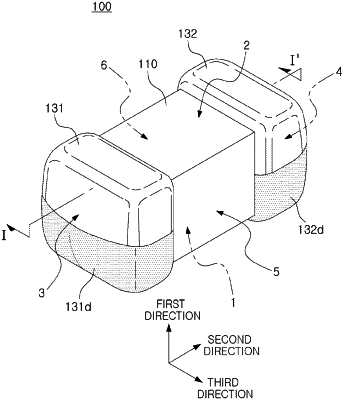
1. A multilayer electronic component comprising:
a body including a dielectric layer and internal electrodes and including first and second surfaces opposing each other in a first direction, third and fourth surfaces connected to the first and second surfaces and opposing each other in a second direction, and fifth and sixth surfaces connected to the first to fourth surfaces and opposing each other in a third direction; and
an external electrode including a connection portion disposed on one of the third and fourth surfaces, an upper band portion extending from the connection portion onto a portion of the second surface, and a lower band portion extending onto a portion of the first surface,
wherein the external electrode includes a Pd plating layer disposed on an external surface of the lower band portion, and the Pd plating layer is disposed to extend onto a portion of the connection portion so as to only partially cover the connection portion, and
wherein a region of an external surface of the external electrode in which the Pd plating layer is not formed is exposed.
|