| CPC H01G 4/1227 (2013.01) [H01G 4/012 (2013.01); H01G 4/0085 (2013.01); H01G 4/30 (2013.01)] | 17 Claims |
|
1. A multilayer ceramic electronic component, comprising:
a ceramic body including a dielectric layer including a grain and first and second internal electrodes stacked in a third direction with the dielectric layer interposed therebetween, and including a first surface and a second surface opposing each other in a third direction, a third surface and a fourth surface opposing each other in a second direction, and a fifth surface and a sixth surface opposing each other in a first direction; and
first and second external electrodes disposed on the fifth surface and the sixth surface of the ceramic body, respectively,
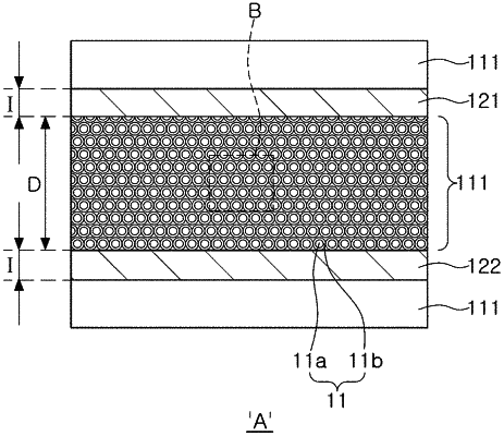
wherein a ratio, G/I, of a particle size, G, of the grain of the dielectric layer to a thickness, I, of each of the first and second internal electrodes is 0.3 or more and less than 0.5,
a thickness, D, of the dielectric layer is five times or more of the particle size, G, of the grain and 20 times or less of the particle size, G, of the grain,
an average thickness of the first and second internal electrodes is 0.4 μm or less, and
a thickness of the ceramic body is 0.8 mm or less.
|