| CPC G11C 29/50004 (2013.01) [G11C 16/0483 (2013.01); G11C 16/08 (2013.01); G11C 16/10 (2013.01); G11C 16/24 (2013.01); G11C 16/3459 (2013.01); H01L 24/08 (2013.01); H01L 25/0657 (2013.01); H01L 25/18 (2013.01); H10B 41/27 (2023.02); H10B 43/27 (2023.02); G11C 2029/5004 (2013.01); H01L 2224/08145 (2013.01); H01L 2924/1431 (2013.01); H01L 2924/14511 (2013.01)] | 20 Claims |
|
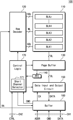
1. A nonvolatile memory device comprising:
a memory cell array including cell strings, wherein each of the cell strings includes a ground selection transistor, memory cells, and a string selection transistor stacked in a direction perpendicular to a substrate;
a row decoder connected with the ground selection transistor of each of the cell strings through a ground selection line, connected with the memory cells of each of the cell strings through word lines, and connected with the string selection transistor of each of the cell strings through a string selection line; and
a page buffer connected with the cell strings through bit lines,
wherein, in a first period of a check operation, the page buffer is configured to apply a first bias voltage to the bit lines,
wherein, in the first period of the check operation, the row decoder is configured to apply a turn-off voltage to the ground selection line, to apply a turn-on voltage to the string selection line, and to apply a first check voltage to the word lines,
wherein, in a second period of the check operation, the page buffer is configured to sense first changes of voltages of the bit lines, and
wherein, in the second period of the check operation, a status fail signal is output in response to that the first changes of the voltages of the bit lines are sensed.
|