US 11,742,040 B2
Nonvolatile memory including on-die-termination circuit and storage device including the nonvolatile memory
Eun-Ji Kim, Suwon-si (KR); Jung-June Park, Seoul (KR); Jeong-Don Ihm, Seongnam-si (KR); Byung-Hoon Jeong, Hwaseong-si (KR); and Young-Don Choi, Seoul (KR)
Assigned to SAMSUNG ELECTRONICS CO., LTD., Suwon-si (KR)
Filed by SAMSUNG ELECTRONICS CO., LTD., Suwon-si (KR)
Filed on Mar. 25, 2022, as Appl. No. 17/704,345.
Application 17/704,345 is a continuation of application No. 17/161,995, filed on Jan. 29, 2021, granted, now 11,342,038.
Application 17/161,995 is a continuation of application No. 16/862,624, filed on Apr. 30, 2020, granted, now 11,024,400, issued on Jun. 1, 2021.
Application 16/862,624 is a continuation of application No. 16/458,933, filed on Jul. 1, 2019, granted, now 10,559,373, issued on Feb. 11, 2020.
Application 16/458,933 is a continuation of application No. 16/426,391, filed on May 30, 2019, granted, now 10,679,717, issued on Jun. 9, 2020.
Application 16/426,391 is a continuation of application No. 15/977,553, filed on May 11, 2018, granted, now 10,340,022, issued on Jul. 2, 2019.
Claims priority of provisional application 62/506,641, filed on May 16, 2017.
Claims priority of application No. 10-2017-0121313 (KR), filed on Sep. 20, 2017.
Prior Publication US 2022/0215892 A1, Jul. 7, 2022
This patent is subject to a terminal disclaimer.
Int. Cl. G11C 7/10 (2006.01); G11C 16/06 (2006.01); G11C 29/02 (2006.01); G11C 5/06 (2006.01); G11C 16/26 (2006.01); G11C 16/10 (2006.01)
CPC G11C 29/025 (2013.01) [G11C 5/063 (2013.01); G11C 7/1048 (2013.01); G11C 7/1057 (2013.01); G11C 7/1084 (2013.01); G11C 16/06 (2013.01); G11C 16/102 (2013.01); G11C 16/26 (2013.01); G11C 29/022 (2013.01); G11C 29/028 (2013.01)] 20 Claims
OG exemplary drawing
 
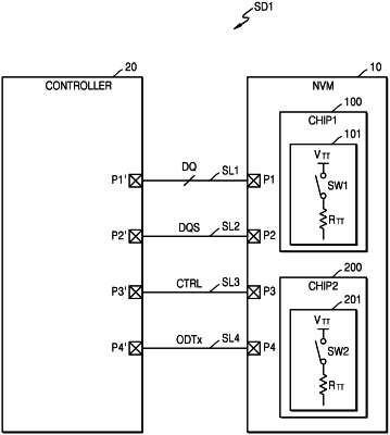
1. A memory system comprising:
a nonvolatile memory (NVM) including a first NVM chip and a second NVM chip; and a controller configured to control the NVM,
wherein the controller comprises:
a data pin configured to receive read data through a data bus during a read operation;
a data strobe pin configured to receive a data strobe signal through a data strobe signal bus during the read operation;
a read enable pin configured to transmit a read enable signal through a read enable signal bus during the read operation, the read enable signal comprising a preamble section, a toggling section and a postamble section; and
an on-die termination (ODT) pin configured to transmit an ODT signal during the read operation,
wherein the ODT signal enables and disables termination on at least one of the data bus, the data strobe signal bus, and the read enable signal bus of the NVM, wherein the termination is enabled during the preamble section of the read enable signal after the read enable signal falling, and the termination is disabled during the postamble section of the read enable signal, wherein the first NVM chip includes a first ODT circuit, and the first ODT circuit is used to perform the ODT when the read data is read from the second NVM chip.