US 11,742,033 B2
Voltage generation circuit which is capable of executing high-speed boost operation
Tatsuro Midorikawa, Kamakura (JP); and Masami Masuda, Chigasaki (JP)
Assigned to Kioxia Corporation, Tokyo (JP)
Filed by Kioxia Corporation, Tokyo (JP)
Filed on Jan. 10, 2022, as Appl. No. 17/647,509.
Application 17/647,509 is a continuation of application No. 17/031,656, filed on Sep. 24, 2020, granted, now 11,250,919.
Application 17/031,656 is a continuation of application No. 16/670,862, filed on Oct. 31, 2019, granted, now 10,818,364, issued on Oct. 27, 2020.
Application 16/670,862 is a continuation of application No. 16/273,979, filed on Feb. 12, 2019, granted, now 10,515,706, issued on Dec. 24, 2019.
Application 16/273,979 is a continuation of application No. 15/417,489, filed on Jan. 27, 2017, granted, now 10,242,748, issued on Mar. 26, 2019.
Application 15/417,489 is a continuation of application No. 14/257,501, filed on Apr. 21, 2014, granted, now 9,589,656, issued on Mar. 7, 2017.
Application 14/257,501 is a continuation of application No. 13/235,437, filed on Sep. 18, 2011, granted, now 8,755,235, issued on Jun. 17, 2014.
Claims priority of application No. 2010-245285 (JP), filed on Nov. 1, 2010.
Prior Publication US 2022/0130471 A1, Apr. 28, 2022
Int. Cl. G11C 16/30 (2006.01); H02M 3/07 (2006.01)
CPC G11C 16/30 (2013.01) [H02M 3/07 (2013.01)] 8 Claims
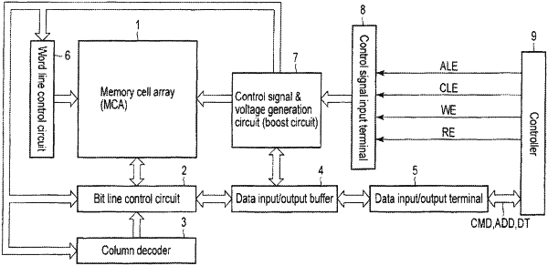
OG exemplary drawing
 
1. A voltage generation circuit comprising:
a charge pump circuit configured to output a first voltage;
a voltage division circuit configured to divide the first voltage to a second voltage;
a first amplifier having a first input terminal and a second input terminal, the first input terminal of the first amplifier configured to receive the second voltage, the second input terminal of the first amplifier configured to receive a third voltage, the first amplifier configured to output a signal which controls the charge pump circuit; and
a capacitor having a first end connected to an output terminal of the charge pump circuit and a second end connected to the first input terminal of the first amplifier via a first transistor.