| CPC G11C 16/30 (2013.01) [G11C 16/0483 (2013.01); G11C 16/24 (2013.01); G11C 16/26 (2013.01)] | 20 Claims |
|
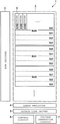
1. A semiconductor memory device comprising:
a memory cell array including:
a first memory string including a first select transistor, a first memory cell transistor connected in series with the first select transistor, and a second memory cell transistor connected in series with the first memory cell transistor; and
a second memory string including a second select transistor, a third memory cell transistor connected in series with the second select transistor, and a fourth memory cell transistor connected in series with the third memory cell transistor;
a first word line connected to a gate of the first memory cell transistor and a gate of the third memory cell transistor;
a second word line connected to a gate of the second memory cell transistor and a gate of the fourth memory cell transistor;
a first selection gate line connected to a gate of the first select transistor;
a second selection gate line connected to a gate of the second select transistor;
a bit line connected to one end of the first memory string and one end of the second memory string; and
a source line connected to the other end of the first memory string and the other end of the second memory string,
wherein, during a read operation performed on the first memory cell transistor,
the second word line is boosted from a first voltage to a second voltage over a first time interval starting at a first time point and ending at a second time point, thereafter further boosted from the second voltage to a third voltage over a second time interval starting at the second time point and ending at a third time point, and thereafter maintained at the third voltage over a third time interval starting at the third time point and ending at a fourth time point,
the first selection gate line is boosted from the first voltage to the second voltage over the first time interval starting at the first time point,
the first word line is boosted from the first voltage to a fourth voltage, which is lower than the second voltage, over a fourth time interval, which is shorter than the first time interval, starting at the first time point and ending at a fifth time point, and thereafter set to a fifth voltage lower than the fourth voltage, and
the second selection gate line is boosted from the first voltage to a sixth voltage, which is lower than the second voltage, over the fourth time interval starting at the first time point, and thereafter decreased to a seventh voltage lower than the sixth voltage.
|