| CPC G11C 16/26 (2013.01) [G11C 7/06 (2013.01); G11C 11/5628 (2013.01); G11C 11/5642 (2013.01); G11C 11/5671 (2013.01); G11C 16/10 (2013.01); G11C 16/3459 (2013.01); H10B 43/27 (2023.02); H10B 43/35 (2023.02); G11C 7/1039 (2013.01); G11C 16/0483 (2013.01); G11C 2211/562 (2013.01); G11C 2211/563 (2013.01); G11C 2211/5621 (2013.01); G11C 2211/5641 (2013.01); G11C 2211/5642 (2013.01)] | 12 Claims |
|
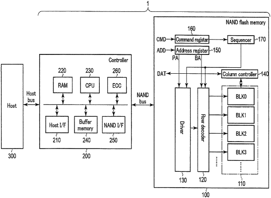
1. A memory system comprising:
a semiconductor memory configured to store data; and
a controller configured to control the semiconductor memory,
wherein the semiconductor memory includes:
a plurality of first blocks each including a memory cell configured to store data of at least one bit,
a second block including a memory cell configured to store data of two or more bits, and
a sense amplifier including a first latch circuit and a second latch circuit,
wherein data is written into the semiconductor memory in units of a page by both a first write operation and a second write operation,
wherein in the first write operation,
the controller outputs a first write command specifying first data, a second write command specifying second data, and a third write command,
the semiconductor memory writes the first data into a first one of the first blocks, and the second data into a second one of the first blocks, and when receiving the third write command, the semiconductor memory writes data of at least two pages into the second block, using the first data and the second data,
wherein in the second write operation,
after issuing the third write command, the controller issues a first read command, a second read command, and a fourth write command, and
the semiconductor memory: reads the first data from the first one of the first blocks to the first latch circuit in response to the first read command; reads the second data from the second one of the first blocks to the second latch circuit in response to the second read command; and overwrites data of at least two pages in the second block written by the first write operation in response to the fourth write command, using the first data and the second data that are read to the first latch circuit and the second latch circuit, respectively,
wherein the fourth write command corresponds to a word line selected in response to the third write command,
a verify voltage that is used when the data of at least two pages is written in response to the fourth write command is higher than a verify voltage that is used when the data of at least two pages is written in response to the third write command, and
each of the first data and the second data includes each of a first bit and a second bit of the data of two or more bits to be written in the memory cell of the second block.
|