| CPC G11C 16/14 (2013.01) [G06F 11/076 (2013.01); G06F 11/0727 (2013.01); G11C 13/00 (2013.01); G11C 16/12 (2013.01); G11C 16/3459 (2013.01); G11C 11/5635 (2013.01); G11C 11/5671 (2013.01); G11C 16/0483 (2013.01)] | 20 Claims |
|
1. A system comprising:
a memory array including memory cells; and
a processing device coupled to the memory array, the processing device to perform operations comprising:
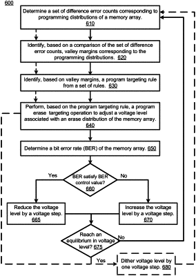
selecting a program targeting rule based on values of a plurality of valley margins of programming distributions of the memory array;
performing, using the program targeting rule, a program erase targeting operation to adjust a voltage level associated with an erase distribution of the memory array;
determining a bit error rate (BER) of the memory array; and
in response to the BER not satisfying a BER control value, increasing the voltage level by a voltage step.
|