| CPC G11C 16/10 (2013.01) [G06F 3/061 (2013.01); G06F 3/0658 (2013.01); G06F 3/0659 (2013.01); G06F 3/0679 (2013.01); G11C 16/0483 (2013.01); G11C 11/5628 (2013.01)] | 13 Claims |
|
1. A memory system comprising:
a memory chip that includes:
a first word line,
a first plurality of memory cells connected to the first word line, each of the first plurality of memory cells being configured to store a plurality of bits of data corresponding to a plurality of threshold voltages,
a second word line, and
a second plurality of memory cells connected to the second word line, each of the second plurality of memory cells being configured to store a plurality of bits of data corresponding to the plurality of threshold voltages; and
a memory controller configured to perform a first write operation, a second write operation after the first write operation, a third write operation after the second write operation, and a fourth write operation after the third write operation, wherein
the first write operation includes transmitting a first command sequence to the memory chip to cause the memory chip to execute a first-stage program operation on the first plurality of memory cells,
the second write operation includes transmitting the first command sequence to the memory chip to cause the memory chip to execute the first-stage program operation on the second plurality of memory cells,
the third write operation includes transmitting a second command sequence to the memory chip to cause the memory chip to execute a second-stage program operation on the first plurality of memory cells,
the fourth write operation includes transmitting the second command sequence to the memory chip to cause the memory chip to execute a second-stage program operation on the second plurality of memory cells,
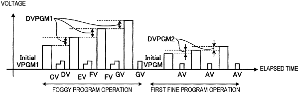
the first-stage program operation includes a first operation and a first part of a second operation after the first operation,
the second-stage program operation includes a second part of the second operation and no part of the first operation,
the first operation includes applying a program voltage a plurality of times while increasing the program voltage each of the times by a first step size, and
the first part of the second operation includes applying the program voltage a plurality of times while increasing the program voltage each of the times by a second step size smaller than the first step size.
|