| CPC G11C 13/004 (2013.01) [G11C 13/003 (2013.01); G11C 13/0028 (2013.01); G11C 13/0069 (2013.01)] | 20 Claims |
|
1. A storage device, comprising:
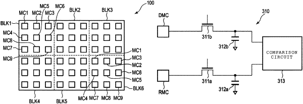
a memory cell array in which a plurality of memory cells respectively including a variable resistance memory element are divided into a plurality of memory blocks, the plurality of memory cells including a first memory cell and a second memory cell that are in the same memory block; and
a detection circuit, wherein
during a read operation in which the first memory cell is a read target, the detection circuit compares a first resistance value, which is a resistance value of the variable resistance memory element in the first memory cell, with a second resistance value, which is a resistance value of the variable resistance memory element in the second memory cell, and determines a value of data stored in the first memory cell based on whether or not the first resistance value is higher or lower than the second resistance value.
|