| CPC G11C 11/4091 (2013.01) [G11C 7/08 (2013.01); G11C 16/06 (2013.01); G11C 16/24 (2013.01); G11C 16/26 (2013.01); G11C 7/1057 (2013.01); G11C 16/0483 (2013.01)] | 6 Claims |
|
1. A memory device, comprising:
a memory block for storing data;
page buffers coupled to the memory block through bit lines; and
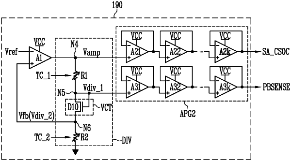
a signal generator configured to output a common sensing signal and a sensing signal included in page control signals for controlling the page buffers in response to an amplified voltage and a divided voltage generated through a single feedback loop,
wherein the page buffers are configured to precharge the bit lines, or sense a voltage or current in the bit lines in response to the page control signals including the common sensing signal and the sensing signal, and
wherein the signal generator comprises a divider circuit including at least one variable resistor and a voltage regulator, and configured to divide the amplified voltage to generate the divided voltage and a feedback voltage of the single feedback loop by the at least one variable resistor and the voltage regulator.
|