| CPC G11C 11/405 (2013.01) [G06F 12/0893 (2013.01); H01L 27/1225 (2013.01); H10B 12/00 (2023.02)] | 4 Claims |

|
1. A semiconductor device comprising:
a memory device and a control circuit,
wherein the memory device comprises a first memory circuit configured to be operated in a first memory level and a second memory circuit configured to be operated in a second memory level,
wherein the first memory level is a level with a higher access speed than the second memory level,
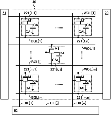
wherein the first memory circuit comprises a first transistor and the second memory circuit comprises a second transistor,
wherein each of the first transistor and the second transistor comprises an oxide semiconductor layer, a first gate and a second gate overlapped with the first gate, and
wherein the control circuit is configured to input a voltage to the second gate of the first transistor so that the first memory circuit is changed from the first memory level to the second memory level, and to input a voltage to the second gate of the second transistor so that the second memory circuit is changed from the second memory level to the first memory level.
|